When you have more than one PCI host bridge/PCI Express root complex in a system, such as a modern high end multi socket board (each processor package usually has an integrated PCIe root complex these days), an interesting set of problems comes into play:
- Each host bridge must respond to a unique range of bus numbers for configuration space accesses. It must know the bus number on the other side of it and the highest bus number below it (the subordinate bus number). In single host bridge systems, the first is zero by default and the latter doesn’t matter.
- Each host bridge must respond to a unique range of memory and I/O addresses on the host bus to pass on to the PCI(e) fabric behind them. For modern Intel systems with a single root complex, the PCI address range is usually subtractively decoded (whatever addresses are ‘left over’ unclaimed by other targets are forwarded to PCI). This, obviously, cannot work when you have more than one host bridge because you now have to decide exactly which addresses are allocated to which host bridge.
The first restriction applies only when both host bridges implement their PCI Configuration Address/Data or the base address of their enhanced configuration mechanism at the same address. But I haven’t come accross a system yet that actually implements them at different addresses. Initialising the system properly while keeping these restrictions in mind is the job of the firmware (at least on x86). I was curious about how exactly this is done and wanted to see it in action with an actual system. I didn’t get too far with modern PCIe systems. You might find a register here and there that is relevant in the datasheets that Intel provides for its high end Xeon processors that are used in multi socket systems, but they will leave you with more questions than before. I also found a paper discussing address decoding on Xeon CPUs, but it focused more on DRAM and not PCIe. The thing is, address decoding on modern server level systems is very complex. In old PCI based Pentium systems, all processors interfaced with the memory controller on the chipset through a common front side bus. Today, you have memory controllers integrated into the processor package, requiring other solutions based on more complex topologies such as rings and meshes, such as Intel’s QPI (Quick Path Interconnect) and UPI (Ultra Path Interconnect). To make things even more complex, each processor package also has a PCIe root complex and a separate logical PCI bus for configuration purposes. The result is that decoding information from whatever little documentation Intel provides for these systems is next to impossible.
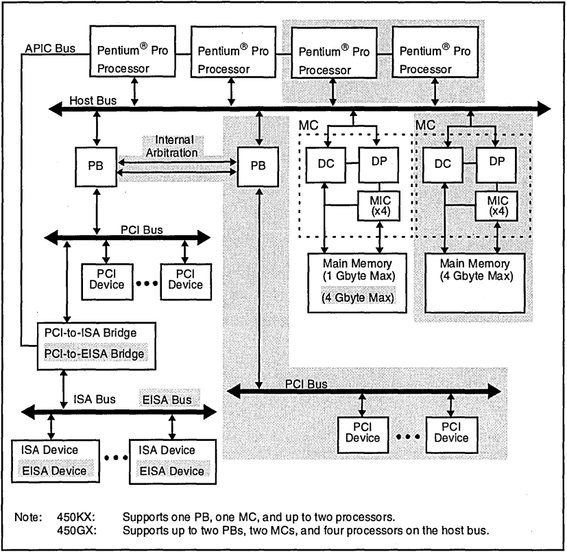
By contrast, it is quite simple to understand old multi socket PCI based Pentium systems. I found a relatively thorough description of the exact aspects discussed above in the datasheet for Intel’s old (as old as 1996) 450 KX/GX “PCIset” chipset. This chipset supports upto four Pentium Pro processors, two PCI host bridges (the GX variant) and two memory controllers:
How, then, are the various aspects mentioned above managed in this chipset? First, let’s talk about how PCI configuration space accesses are handled.
Configuration Space
To allow software to configure bus numbers, memory address ranges, IO address ranges and other aspects, the two bridges expose themselves as PCI devices residing on PCI bus 0. In fact, not just the bridges, but also the memory controller is mapped as a PCI device on bus 0. These ‘pseudo - PCI’ devices use device numbers greater than 15, whereas numbers below 15 are free and are mapped to a unique AD[31:16] line (more on mapping of device numbers to AD lines, IDSEL# etc. later) so that the hierarchy below a PCI bridge can begin with bus zero. For example, on reset, the first PCI host bridge (PB from hereon), also referred to as the compatibility PB since it has a PCI to ISA bridge below it, is assigned a device number of 25, whereas the other PB, referred to as the Auxiliary PB is assigned a device number of 26. Here is a description of how the two bridges behave after reset and after proper configuation -
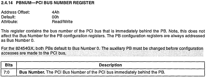
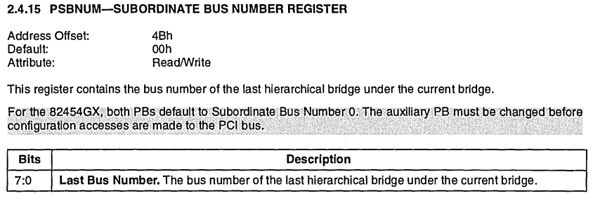
- Firstly, both host bridges implement a register to change the bus number on their secondary side and the subordinate bus number for the buses below them:
- At reset, both of these values are zero. This might not make sense at first because you might think both bridges will respond to configuration accesses to bus number zero. However, only the compatibility PB acts as the response agent for the transaction. If the device number is greater than 15 and matches its own device number, it responds to the transaction itself. The auxiliary PB simply snarfs the data being written to the configuration address register, and if the bus number is zero with the device number matching its own, it will respond to the transaction instead. If the bus number is zero but the device number less than 16, it is the compatibility PB that generates a configuration cycle on the PCI bus behind it. In this way, there is a unique responder to each type of configuration access on reset.
- Once the firmware has discovered all the devices and buses behind the compatibility PB, it will set the subordinate bus number for the compatibility PB and the primary bus number for the auxiliary PB, which will cause the auxiliary PB to start responding to configuration accesses targeted to devices with device number below 15, thus enabling firmware to discover all the devices and buses behind the auxiliary PB.
After firmware allocates bus numbers, operating systems/bootloaders can discover PCI devices normally.
Memory and IO Regions
In systems with a single host bridge/root complex, the address space that is ‘left over’/ not decoded by any other devices is allocated to the PCI/PCIe bus. For example, the region between the last address allocated to DRAM below 4G to 4G, excluding the space allocated for the IOAPIC registers, or the region between the last address allocated to DRAM and the very top of the physical address space (called ‘High MMIO’). In systems with multiple host bridges though, specific regions have to be allocated to each host bridge. In the 82454GX host bridge, specific regions can be programmed to be positively decoded to PCI:
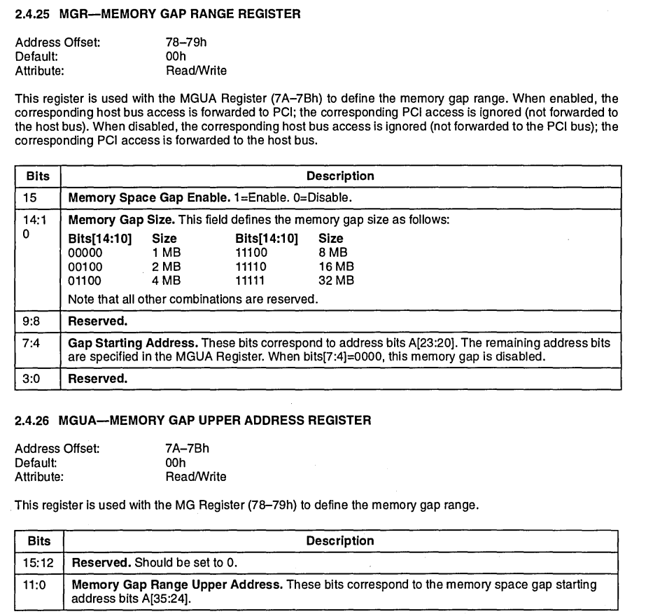
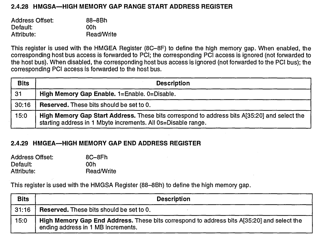
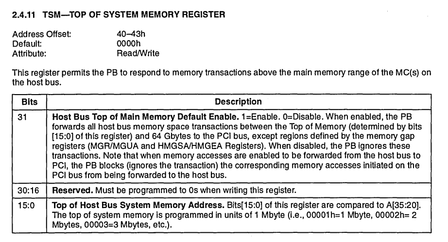
These ranges are disabled by default and have to be programmed. In addition, the compatibility PB decodes all addresses from the top of system memory to 64G, if enabled:
There are similar registers to configure I/O space regions.
What is a PCI device number really?
How are PCI deveces assigned device numbers? Firstly, bus/device/function numbers matter only during configuration transactions. The PCI specification defines the IDSEL signal to select devices during configuration transactions. When a PCI device sees its IDSEL signal asserted during a configuration transaction (the command is configuration read/write on C/BE[3:0]), it knows that it is the target of the transaction. If it is, it decodes the following information about the transaction from the AD signals:
AD[1:0]indicates the type of the transaction. A value of 00 indicates type 0, a transaction targeting a device on this bus.AD[7:2]indicates which dword of the configuration space is being accessed.AD[10:8]selects one of 8 functions in the device.AD[31:11]are reserved and are not decoded by the devices.
The last point lends itself to an easy way to implement the IDSEL signal. The host bridge can simply assert one of the twenty AD[31:11] lines for a specific device number. The board designer can then connect IDSEL to that line on the PCI slot.
For an example of this in action, let us consider the ICH-3 southbridge chipset, for which Intel has a platform design guide that contains reference schematics. In section 5.1.3 (IDSEL to Device number mapping), it says the following:
- When addressing devices on the external PCI bus (with the PCI slots) the ICH3 will assert one address signal as an IDSEL. When accessing device 0, the ICH3 will assert AD16. When accessing Device 1, the ICH3 will assert AD17. This mapping continues all the way up to device 15 where the ICH3 asserts AD31.
This tells us how device numbers are mapped to AD lines by the chipset. Let us now look at the board schematics from the platform design guide that will tell us how the IDSEL signals for each PCI slot are connected to AD lines:
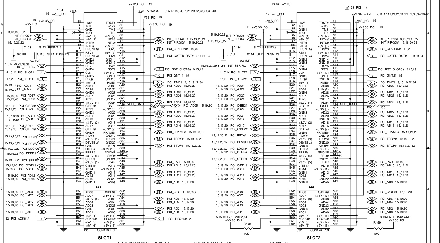
The IDSEL of slot 1, pin A26 in the above schematic, is connected to PCI_AD25, that is AD25. The IDSEL of slot 2 is connected to PCI_AD26, that is AD26. From the ICH3 datasheet we know that AD25 and AD26 will be driven when a configuration cycle targeting device 9 and 10 is being generated. That means devices connected to slot 1 and slot 2 will be discovered with device numbers 9 and 10 respectively. Usually device numbers 0-15 are mapped as such and higher device numbers are decoded to devices internal to the chipset.
The other way to implement the IDSEL signal is to route separate traces on the board, but that is of course not as neat.