The PCI local bus specification defines four active low, level trigerred interrupt signals - INT[A-D]# per device. On x86 machines, you have the IOAPIC and legacy 8259 interrupt controllers. The 8259 has effectively 15 interrupt pins, and the IOAPIC usually has somewhere between 19-24 pins, with the possibility of having more than one in a chipset. To install an interrupt handler for a PCI device, you need to find out which pin the device is using, and to which pin on the 8259 or IOAPIC it is connected. How would you do this?
On very old, pre-ACPI systems you had the traditional PCI BIOS - access is provided to the routines through real mode interrupt vectors - int 1AH. I’ll skip over this since it is irrelevant today, but the essence is that there is are routines to get and set interrupt routing information given a PCI bus and device number. This method is defined only for 8259 controllers, possibly because it predates the existence of the IOAPIC. Note that you can set interrupt information - meaning the interrupt pin of the 8259 that the interrupt is routed to is configurable - this is true even for the legacy 8259s included in today’s chipsets. You can find the details of this method in the PCI firmware specification.
For systems with ACPI, the DSDT includes a device for every host bridge/root complex present on the system. Under this device, you have a method called _PRT, or PCI Routing Table, that includes interrupt information for devices on the root bus corresponding to this particular host bridge. The information returned by this method varies depending on whether you want routing information for the legacy 8259 PIC or for the IOAPIC(s). To declare which one you are looking for, execute the _PIC method. Usually this method saves your preference in a global variable and then this variable is used when calling _PRT. Let us look at a part of the information returned by _PRT when you have already called _PIC requesting information for the IOAPIC:
1
2
3
4
5
6
7
8
9
10
11
12
13
14
15
16
17
18
19
20
21
22
23
24
25
26
27
28
29
30
31
Package (0x04)
{
    0x001CFFFF,
    0x00,
    0x00,
    0x10
},

Package (0x04)
{
    0x001CFFFF,
    0x01,
    0x00,
    0x11
},

Package (0x04)
{
    0x001CFFFF,
    0x02,
    0x00,
    0x12
},

Package (0x04)
{
    0x001CFFFF,
    0x03,
    0x00,
    0x13
},
This is ACPI AML code, but you don’t need to understand much to see what’s going on here. The ACPI specification defines a format for the information returned by _PRT - each package must have:
- A DWORD for the address of the device - for PCI devices the upper word contains the device number and the lower word contains the function number. A function number of
0xFFFF(an invalid function number as PCI defines only 8 functions per device) indicates ‘any device’. - A Byte indicating which pin -
0x0isINTA#and0x3isINTD#. - Either a NamePath or a Byte. If it is a NamePath, it indicates a device in the ACPI namespace which whill allocate the interrupt - a programmable interrupt router. If it is a Byte, it has to be zero and indicates that the interrupt is fixed and cannot be configured.
- A DWORD that is defined only if the Byte in the previous field is zero. This indicates the GSI (global system interrupt) that the interrupt is routed to. The ACPI specification defines GSIs as follows - to get the pin of an IOAPIC that the interrupt is connected to, subtract the GSI base for the IOAPIC (can be found in the MADT) from the GSI. Meaning, if you have two IOAPICs with 24 pins, they might be indicated in the MADT as having GSI bases of 0 and 24, and so when you encounter a GSI of 40, it really means pin 16 of the second IOAPIC.
In the above piece of code, take the first package - if you apply the above format you get to know that the INTA pin of device 0x1c (bus 0 in this case since I took this out of the _PRT of the only host bridge on this system) is connected to GSI 0x10. On this system, the MADT indicated that there is only one IOAPIC with a GSI base of zero, so this is really pin 16 of the only IOAPIC of the system. So you can program the corresponding redirection entry in the IOAPIC’s configuration registers with the vector and LAPIC ID of your choice and install your interrupt handler for that vector, and your job is done. Your interrupt handler will be called everytime this device drives its INTX# pin.
What if, for whatever reason, you want to use the legacy 8259 PIC? The package returned by _PRT will look like this -
1
2
3
4
5
6
7
8
9
10
11
12
13
14
15
16
17
18
19
20
21
22
23
24
25
26
27
28
29
30
31
Package (0x04)
{
    0x001CFFFF,
    0x00,
    \_SB.LNKA,
    0x00
},

Package (0x04)
{
    0x001CFFFF,
    0x01,
    \_SB.LNKB,
    0x00
},

Package (0x04)
{
    0x001CFFFF,
    0x02,
    \_SB.LNKC,
    0x00
},

Package (0x04)
{
    0x001CFFFF,
    0x03,
    \_SB.LNKD,
    0x00
},
Applying the format defined by the ACPI spec to the first package, we get to know that pin INTA# of device 0x1c is configurable and is allocated by a device called \_SB.LNKA in the ACPI namespace. I’ll include the definition of this device below:
1
2
3
4
5
6
7
8
9
10
11
12
13
14
15
16
17
18
19
20
21
22
23
24
25
26
27
28
29
30
31
32
33
34
35
36
37
38
39
40
41
42
43
44
45
46
47
48
49
50
51
52
53
54
55
56
57
Device (LNKA)
{
    Name (_HID, EisaId ("PNP0C0F") /* PCI Interrupt Link Device */)  // _HID: Hardware ID
    Name (_UID, 0x01)  // _UID: Unique ID
    Method (_STA, 0, NotSerialized)  // _STA: Status
    {
	If (!VPIR (\_SB.PCI0.LPC.PIRA))
	{
	    Return (0x09)
	}
	Else
	{
	    Return (0x0B)
	}
    }

    Name (_PRS, ResourceTemplate ()  // _PRS: Possible Resource Settings
    {
	IRQ (Level, ActiveLow, Shared, )
	    {3,4,5,6,7,9,10,11}
    })
    Method (_DIS, 0, NotSerialized)  // _DIS: Disable Device
    {
	\_SB.PCI0.LPC.PIRA |= 0x80
    }

    Name (BUFA, ResourceTemplate ()
    {
	IRQ (Level, ActiveLow, Shared, _Y00)
	    {}
    })
    CreateWordField (BUFA, \_SB.LNKA._Y00._INT, IRA1)  // _INT: Interrupts
    Method (_CRS, 0, NotSerialized)  // _CRS: Current Resource Settings
    {
	Local0 = (\_SB.PCI0.LPC.PIRA & 0x8F)
	If (VPIR (Local0))
	{
	    IRA1 = (0x01 << Local0)
	}
	Else
	{
	    IRA1 = 0x00
	}

	Return (BUFA) /* \_SB_.LNKA.BUFA */
    }

    Method (_SRS, 1, NotSerialized)  // _SRS: Set Resource Settings
    {
	CreateWordField (Arg0, 0x01, IRA2)
	FindSetRightBit (IRA2, Local0)
	Local1 = (\_SB.PCI0.LPC.PIRA & 0x70)
	Local1 |= Local0--
	\_SB.PCI0.LPC.PIRA = Local1
    }
}
It looks quite a bit more complex, but here’s how it works - you call the _PRS (Possible Resource Settings) method of this device to get the list of all possible IRQs of the 8259 that you can route it to. In this case, you can see that it’s IRQs 3,4,5,6,7,9,10,11. If you want to route it to one of these IRQs, call _SRS (Set Resource Settings) with that IRQ as an argument. To see which IRQ is currently configured, call _CRS (Current Resource Settings). To disable the link, call _DIS and to get the status of the link, call _STA. This is what these methods do. To understand how they do it, and what all that code above means, keep reading.
You will notice that all this information is bus relative, since every package contains only a device number. Every PCI bridge on the system will also have a _PRT method to provide routing information for devices behind that bridge. In case it doesn’t, or the bridge doesn’t exist at all in the ACPI namespace, it means that the interrupt pins for devices behind that bridge are mapped to interrupt pins on the bridge itself in a specific manner. This is the interrupt swizzle defined in the PCI-PCI bridge specification -
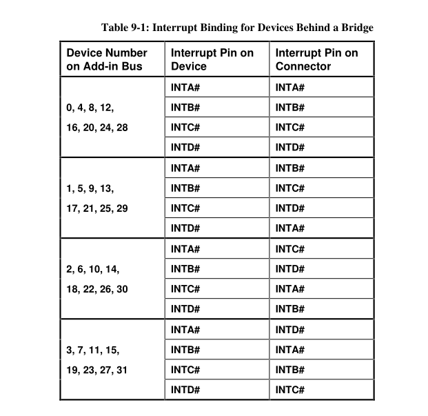
So, given that you have interrupt routing information for the bridge itself, you can get the routing for devices behind the bridge. By now, you should know how to get interrupt routing information for a particular PCI device and exactly how its INTX# pins are routed to the systems interrupt controller. So if your goal is to get PCI interrupts working on your operating system, you should be good to go.
I will now take the example of a specific chipset and show why the routing information provided is what it is. I will use a Thinkpad T420 - it contains a Sandy Bridge Intel Core i5-240M with a Cougar Point Intel C200 PCH chipset. The datasheets for both of these are publicly available, and so I can show you exactly how you can make sense of the interrupt routing information you will find on this machine. First, there are some differences you should understand since this system contains a PCIe fabric and not PCI, although PCIe is compatible with PCI from a software perspective.
PCIe is a point to point interconnect as opposed to the shared bus nature of PCI. To remain compatible with PCI in software, consistency is maintained with the PCI topology as follows - the point to point link is represented as a bus, and the PCIe endpoint at the end of it is device 0. This is why you will notice that on most machines, lspci will display a lot of devices with number 0 and on different buses. A root port presents itself as a PCI-PCI bridge to software, with the bus number of its secondary side (the PCIe link) freely configurable just as in PCI. You will also see devices with non zero device numbers - these are root complex integrated devices - they are present in the chipset or processor package itself and are enumerated as PCI devices, with a hardcoded device number. PCIe also eliminates the four sideband interrupt signals in favour of message signaled interrupts. For software compatibility, a special TLP (Transaction Layer Packet, PCIe is a layered protocol) type is defined - Assert_INTX# and Deassert_INTX. The device generates these transactions if it has been configured to use legacy interrupts. The root complex must keep track of these messages and translate them into an interrupt event at a pin of one of its interrupt controllers.
Now, about the Thinkpad T420 I shall be talking about - the Core i5-240M has a memory controller integrated into the CPU package. This means that the silicon that generates memory transactions on DRAM, generates PCIe configuration transactions, maps address ranges to specific targets is on the processor package itself - functions that were traditionally part of the Northbridge external chipset. This Thinkpad contains the C200 series PCH, or platform controller hub - this is the modern equivalent of the Southbridge and contains various I/O such as xHCI, SATA, PCIe ports etc. The PCH is linked to the processor through DMI (Direct Media Interface). You can think of the DMI as just a logical extension of PCI bus 0. Look at the output of lspci on this system -
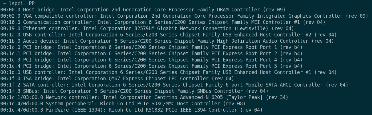
Devices 0 and 2 on PCI bus 0 are part of the processor package, and devices 0x16 through 0x1f are part of the PCH. DMI is essentialy “extending” PCI bus 0, making these devices that are part of separate physical components appear on the same bus. This particular PCH has eight root ports, functions 0-8 of device 0x1c. Only four of them are visible here though, because this chipset provides a way to hide root ports that are unused. Have a look at section 10.1.3 of the PCH datasheet:

Okay, now to the relevant part. If you go through sections 5.8 through 5.10 of the PCH datasheet, you will find that this chipset integrates both a legacy AT compatible 8259 PIC as well as a 24 pin IOxAPIC as part of its interrupt interface. The first 16 legacy interrupt sources such as the RTC, the PIT, the PS/2 controller etc. are mapped 1-1 to the first 16 pins of the IOAPIC, with the exception of the PIT, since the first pin of the IOAPIC is usually connected to the PIC as a cascade. For interrupts from PCIe devices, this PCH defines the PIRQ[A-H]# (PCI/Peripheral IRQ?) signals which can be routed to certain pins of the 8259 PIC, or are connected directly to pins 17-24 of the IOAPIC. Since PCIe INTX interrupts are really just messages and not physical signals, the PCH can route these to the PIRQ[A-H]# signals as it pleases. In fact, look at sections 10.1.28 through 10.1.34 of the PCH datasheet:
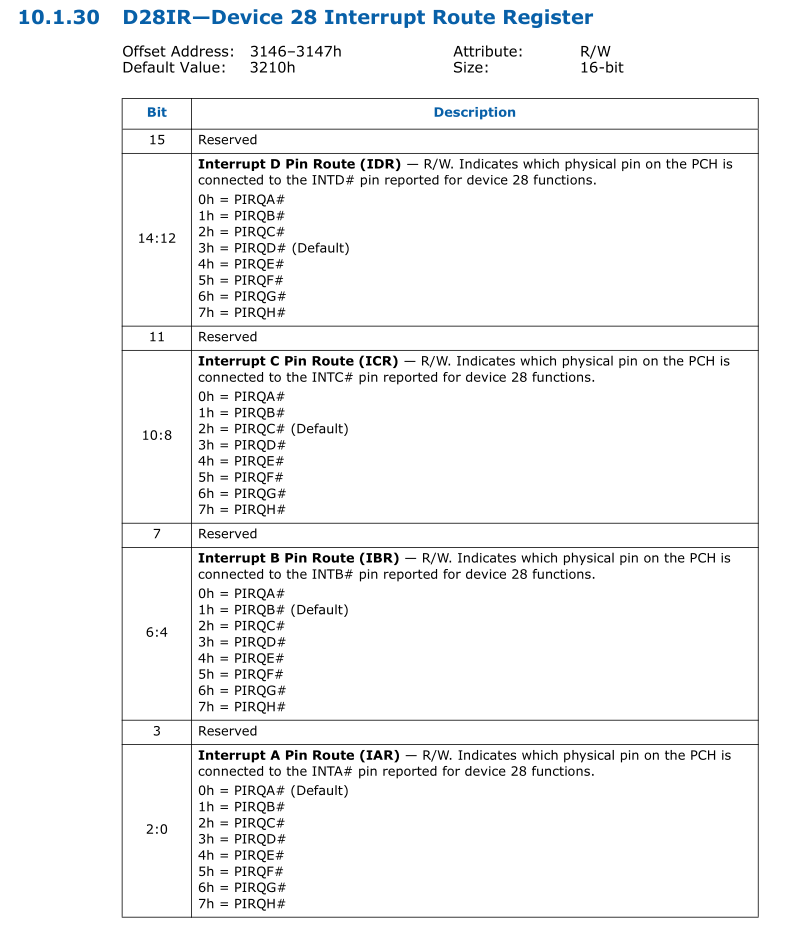
The above register controls how the virtual INTx signals of device 28 are mapped to the chipsets PIRQ[A-H] signals. Recall from the lspci dump above that device 28 contains the root ports of the chipset. Let us try to actually read this register. You can see that this register is at an offset of 3146h from the base of the chipset configuration registers block, whose base address according to the datasheet is in the RCBA (Root Complex Base Address) register of the PCI-LPC bridge. I’ll read this register using the setpci utility, which enables you to read from the configuration space of PCI devices:
1
2
root@t420:~# setpci -s 00:1f.0 F0.L
fed1c001
00:1f.0 is the bus:device.function of the ISA bridge, as you can see in the lspci dump, and F0.L tells setpci to read a [L]ong from offset F0h in the configuration space of the device. Apparently, it has been set to FED1C001h by firmware on this system. Look at the format of this register, from section 13.1.39:

Given that it is aligned on a 16 Kib boundary, the base address is then fed1c000h. Okay, so we need to read at an offset of 3146h from this address, a word that will give us the value of the D28IR register. However, a simple setpci in this case will not suffice, since we are no longer dealing with PCI configuration space. We need a way to read from arbitrary physical memory, and writing a kernel module is the best way, since /dev/mem only exposes the low 1 MiB of address space:
1
2
3
4
5
6
7
8
9
10
11
12
13
14
15
16
17
18
19
20
21
22
23
24
25
26
27
28
29
30
31
32
33
34
35
36
37
38
#include <linux/module.h>
#include <linux/moduleparam.h>
#include <linux/init.h>
#include <linux/kernel.h>
#include <linux/slab.h>
#include <linux/fs.h>
#include <linux/errno.h>
#include <linux/cdev.h>
#include <linux/types.h>
#include <linux/fcntl.h>
#include <linux/mm_types.h>
#include <asm/page.h>
#include <linux/pgtable.h>
#include <asm/pgtable_types.h>
#include <asm/types.h>
#include <asm/smp.h>
#include <linux/highmem.h>
#include <asm/io.h>

/* you definitely don't need so many includes, i've simply copy pasted them from another boilerplate module */

int test_init(void)
{

  void *phys_addr = 0xfed1c000;
  void *virt_addr = ioremap(phys_addr, 16 * (1 << 10));
  u32 test = readw(virt_addr + 0x3146);
  printk("register D28IR: 0x%lx\n", test);
  return 0;
}

void test_exit(void)
{
  iounmap(0xfed1c000);
}

module_init(test_init);
module_exit(test_exit);
I’ve used ioremap instead of virt_to_phys since it is highly unlikely that the kernel has mapped so much physical memory on this system, given that it does not support huge pages. I’ve also omitted any error checking on the return value of ioremap. Loading this module gave the folowing output in the kernel ring buffer:
1
[41079.916787] register D28IR: 0x3210
This register has retained its default value of 3210h. This means that pins INT[A-H]# of device 28 are connected to PIRQ[A-D]# (refer to the description of the D28IR register above.). Let’s look at the _PRT table for the PCIe root complex of this system to see if it matches:
1
2
3
4
5
6
7
8
9
10
11
12
13
14
15
16
17
18
19
20
21
22
23
24
25
26
27
28
29
30
31
Package (0x04)
{
    0x001CFFFF,
    0x00,
    0x00,
    0x10
},

Package (0x04)
{
    0x001CFFFF,
    0x01,
    0x00,
    0x11
},

Package (0x04)
{
    0x001CFFFF,
    0x02,
    0x00,
    0x12
},

Package (0x04)
{
    0x001CFFFF,
    0x03,
    0x00,
    0x13
},
It does! Pins INT[A-D]# according to this table are connected to GSIs 0x10-0x13, which according to the chipset datasheet are directly mapped to PIRQ[A-D]#. So, INT[A-D]# -> PIRQ[A-D]# for device 28, which I stated above by reading chipset registers, is also what is indicated in the ACPI tables of this system. Hopefully now you have a bit of insight as to why these interrupts are routed as they are.
You must also realise that this mapping is valid only for device 28, which is a root port, and not for the devices behind the root port. A root port also has reasons for generating interrupts, such as hotplug events. For devices attached to the root port, the ACPI tables provide a different routing:
1
2
3
4
5
6
7
8
9
10
11
12
13
14
15
16
17
18
19
20
21
22
23
24
25
26
27
28
29
30
31
    Package (0x04)
    {
	0xFFFF,
	0x00,
	0x00,
	0x11
    },

    Package (0x04)
    {
	0xFFFF,
	0x01,
	0x00,
	0x12
    },

    Package (0x04)
    {
	0xFFFF,
	0x02,
	0x00,
	0x13
    },

    Package (0x04)
    {
	0xFFFF,
	0x03,
	0x00,
	0x10
    }
This is the routing for 00:1c.1, which as you may recall from the chipset datasheet and PCI dump above, is root port 2. Can you see some similarities with the swizzle I talked about earlier? It seems the pins INT[A-D]# of the device behind this root port are mapped to pins INTB, INTC, INTD, INTA of the root port itself. It seems that the chipset designers decided to use this swizzle, albeit with the function number of the corresponding root port (1 in this case) instead of the device number behind it (which is always 0 for PCI express). This explanation also checks out for the other root ports on this system.
Although this is a neat explanation, it is important not to read too much into it and apply it to any system you find. The mapping of INTx signals for devices behind root ports is completely arbitrary and need not be mapped to the INTx signals of the root port itself. Especially for systems with two IOAPICs, it would greatly reduce how many of the pins you can actually use and needlessly increase interrupt sharing. On my Thinkpad T14 which contains two IOAPICs, for example, this mapping simply does not exist.
Let us now try to decode the AML code we saw earlier that handles routing of PCI interrupts to the legacy 8259 PIC. Look at registers PIRQ[n]_ROUT of the LPC bridge (section 13.1.16 of the chipset datasheet):
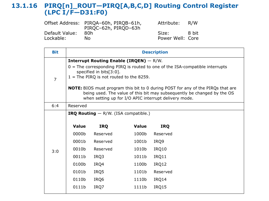
It is fairly straightforward, the highest bit enables or disables the routing and the lower four bits are which pin of the 8259 the interrupt is mapped to. You will realise, then, how the following code, which I said disables the link works:
1
2
3
4
Method (_DIS, 0, NotSerialized)  // _DIS: Disable Device
{
    \_SB.PCI0.LPC.PIRA |= 0x80
}
It is simply turning on the ‘disable’ bit of the relevant configuration register. The other methods, _STA, _CRS, _SRS should also be clear, even though it is quite tedious to read ACPI Source Language code.